Researchers in Materials Research Center of the Institute of Modern Physics, Chinese Academy of Sciences (IMP) have focused on the studies of metal and semiconductor nanowires.Series important results on optical properties of nanowire arrays, controlling the crystal structure of nanowire and preparation of special nano-structure and functional nano-materials have been obtained. Recently, the electrical transport properties of single InSb nanowire were studied, in cooperation with colleagues from Forschungszentrum Jülich, Germany and University of Southern California, USA.
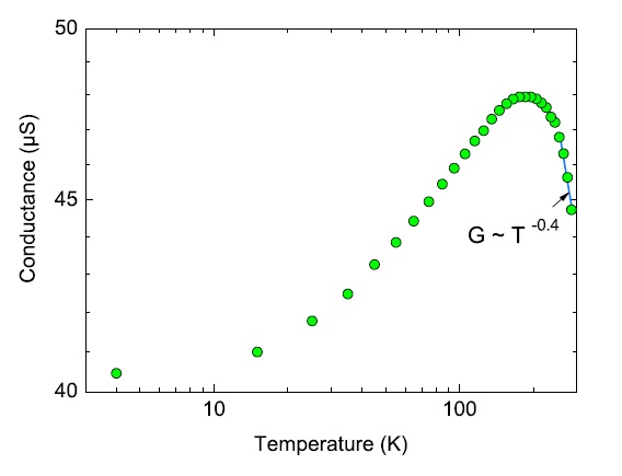
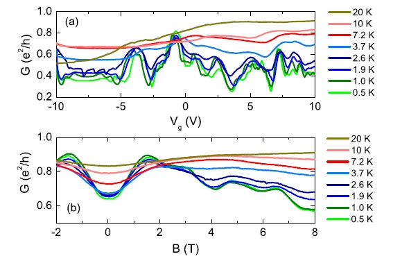
In order to study the electrical properties of single InSb nanowire, the nano-electrodes for nanowire were prepared assisted with electron lithography and the nano-field effect transistors of InSb nanowire were studied. It was confirmed that the 3-dimensional bulk conduction dominates in the nanowire channel after investigating a large number of nanowires with different diameters at room temperature. The transition point from metallic- to semiconductor-like behavior of InSb nanowire was found around 200 K. Strong electron-phonon scattering leads InSb nanowire to exhibit metallic-behavior at higher temperature. Universal conductance fluctuations caused by electron interference was observed through changing the back gate voltage or the applied magnetic field at low temperatures. From the amplitude and the correlation voltage of the conductance fluctuations, the phase-coherence length in InSb nanowires was determined at various temperatures. The phase-coherence length increased with decreasing temperature and saturated at 100 nm when the temperature is lower than 1.9 K.
This work was financially supported by National Natural Science Foundation of China (Nos:11005134, 10805062and 10975164), West Light Project of the Chinese Academy of Sciences and the Natural ScienceFoundation of Gansu Province (1007RJYA014).
The results have been published in Applied Physics Letters, 101, 082103 (2012). The article can be linked as follows: http:/apl.aip.org/resource/1/applab/v101/i8/p082103_s1?bypassSSO=1.

Fig.1. A sketch map for studying electrical transport properties of InSb nanowire and corresponding electron scanning microscope image. (Imaged by IMP)

Fig.2. Temperature dependence of conductance G (Imaged by IMP)

Fig.3. (a) Conductance fluctuations G in units of e2/h as a function of gate voltage at various temperatures in the range from 0.5 to 20 K. (b) Corresponding fluctuations as a function of the magnetic field B. The field is oriented perpendicularly to the wire axis. (Imaged by IMP)

